Apple 3D Printing: Is It Possible to 3D Print an iPhone?

Tech news sites like to regularly report on Apple’s latest patent filings, especially when this comes to such unique technologies as 3D printing. But how feasible is it that a company like Apple or Google could 3D print a smartphone. Could we one day have a 3D printed iPhone? In this article, we’ll explore the possibility that we could one day use additive manufacturing to make advanced electronics, such as smartphones.
There are two ways of going about this: 1. We could imagine a machine that can 3D print large portions of the phone and then pick and place outside objects into the device as it’s being made, or 2. The system could process separate raw materials into a complete device, all within the printer itself.
We’ll start with option one, which, for what are likely obvious reasons, is the more easily achievable of the two.
Factory in a Box
The first scenario might look something like a factory in a box. We could imagine one of our traditional 3D printers—whether it be material extrusion, inkjet, or some other method—make the majority of the phone’s body, perhaps including some electronics. Then, an integrated pick-and-place system could grab all of the necessary functional parts—microchips, camera modules, speakers, etc.—and insert them in their proper positions before they are fused using some mechanism.
Before spinning out into the startup Inkbit, an MIT project demonstrated the possibility of this scenario quite well. Back then, the 3D printer was referred to as MultiFab and it was capable of inkjet 3D printing around prefabricated, functional parts, such as LEDs and lenses. The key to the process, and likely any sort of iPhone making robot we might conceive of here, was machine vision, which was able to recognize these outside parts and work around them.
Inkbit is not primarily focused on this factory-in-a-box solution but is developing all of the necessary tools to make it possible if that is what a customer is looking for. All that’s missing would be an integrated pick-and-place or robotic arm system that could retrieve the additional elements and integrate them into the builds as they’re performed.
Such projects have already been explored. This includes the Industrial Revolution III 3D printer that was able to autonomously integrate prefab wheels and motors into a 3D printed car and BotFactory develops systems capable of laying down solder paste and performing pick-and-place of electronic components for fabricating printed circuit boards (PCBs). The technology works well enough for the U.S. Air Force, which last year awarded BotFactory a grant to create a completely automated PCB 3D printer.
3D Printing an iPhone from Scratch
The above scenario is much more feasible, given that not every single element of a smartphone would have to be made within the 3D printer itself. To continue our thought experiment, however, let’s explore the possibility that every element of the device could be made within a single machine.
Touchscreen
The capacitive touchscreen of modern smartphones are typically made up of an organic light-emitting diode (OLED) display, followed by a glass substrate that acts as an insulator, a coating of transparent conducting material like indium tin oxide or silver, which is then bonded with a protective layer. How close are we to 3D printing any of this stuff?
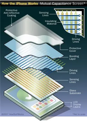
Image courtesy of How Stuff Works.
OLED Display
Interestingly, there are a number of research endeavors working to 3D print varieties of LED screens. Most recently, researchers from the University of Minnesota Twin Cities were able to produce a flexible, 64-bit OLED display using a customized 3D printer. The process primarily relied on using pneumatic dispensers to deposit drops of material for each layer, save one step that relied on an aerosol spray printing technique to lay down the electroluminescent polymer necessary for light emission.
The team is now working on increasing the resolution from 64 bits, simple enough to animate the word “hello” or a smiley face. They’re also looking to integrate transistors and capacitors into the printing process.
Glass
As for the glass substrate, 3D printing glass is tough, but doable. There have been several approaches to 3D printing objects made from the likes of soda lime, borosilicate and other materials. Typically, they include extruding molten glass at extreme temperatures or laser fusing a photocurable polymer infused with glass nanopowder ink, sometimes at the nano scale. Lawrence Livermore National Laboratory (LLNL) developed a direct ink writing technique for 3D printing silica, but it requires sintering the part in a furnace.
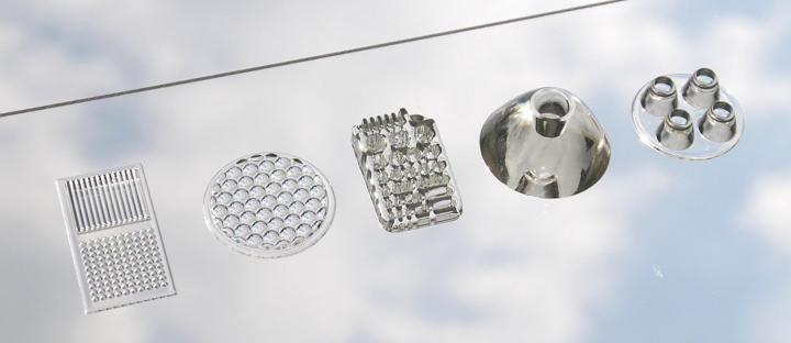
Polymer 3D printed optics made with Luxexcel technology. Image courtesy of Luxexcel.
If glass can be substituted for some other insulating material, such as a transparent plastic, Luxexcel has developed an inkjet technology for 3D printing lenses using an acrylic-based polymer. The company has produced over 50,000 such lenses and is now working on smartglasses, which includes the ability to integrate liquid crystal foils and waveguides into 3D printed prescription lenses.
Electronic Inks
This is an ingredient that has been significantly developed. Multiple companies offer methods for 3D printing conductive materials, particular silver inks. Most notably, Optomec’s Aerosol Jet systems are already used by major smartphone manufacturers to 3D print conductive traces onto parts. The Aerosol Jet machines can spray an ultrafine mist of conductive (silver, gold, platinum, copper), semiconductive, resistor (carbon and ruthenate), and dielectrics (polyimide and polyvinylpyrrolidone) and more onto most substrates, regardless of the shape or complexity.
Otherwise, we might consider technology from Nano Dimension, an inkjet process that can 3D print conductive and dielectric traces within a photopolymer substrate, creating a 3D printed PCB. All that’s left is to add the transistors, capacitors and other elements. nScrypt is able to combine a variety of tasks into a single machine, including microdeposition of conductive materials and integration of electronic components with a pick-and-place head.
Chips
Key to the operation of a smartphone are the ICs and related hardware components, including the processor, memory, accelerometer, gyroscope, power amplifier, flash memory, near-field communications, and wi-fi.
All of these pieces are made up of their individual elements but involve overlapping techniques and materials. For instance, they all require PCBs, which then connect all of the smaller electronic components, such as the ICs, transistors, capacitors, and resistors. We can pretend the technologies described in the above section dedicated to conductive inks could produce the PCBs necessary for each of the modules we’re now discussing.
However, before any of these technologies are ready to 3D print smartphone circuitry, they will need to achieve greater resolution. None are capable of feature sizes necessary for producing integrated circuits (ICs), which require resolution of less than one micron. Instead, Aerosol Jet is limited to 10 microns; nScrypt 20 microns; and Nano Dimension 18 microns. For this reason, Nano Dimension Applications Manager Ziv Cohen suggests that lithography, currently used for IC production, may aid in achieving the proper feature sizes for ICs.
But what about the ICs, transistors, capacitors, and resistors that are mounted onto the PCBs? Believe it or not, all of this has been tried before with some success, as well. In 2015, researchers from the University of California, Berkeley, were able to 3D print a crude inductor–capacitor-resonant tank circuitry with a resonance frequency at 0.53 GHz, as well as smart bottle cap embedded with inductor–capacitor tank and wireless passive sensor to monitor the quality of milk and juice. It involved a simple fused deposition modeling (FDM) 3D printer and sacrificial (support) material that was then rinsed out and replaced with liquid metal paste to create the circuitry.
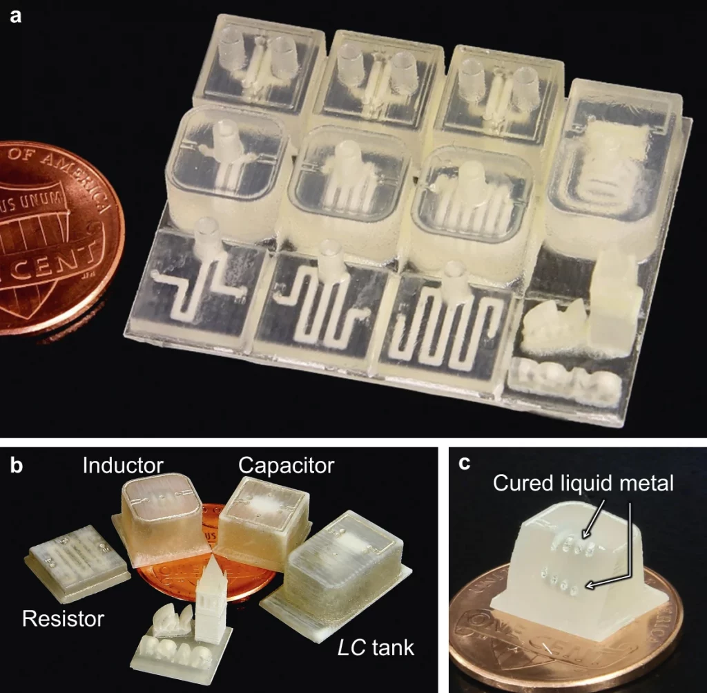
(a) An optical image showing fabricated microelectronics components produced using the 3D printing process without the embedded conductive structure compared with a one-cent US coin. (b) Fabricated 3D components, including resistors, inductors, and capacitors, and an LC tank after the liquid metal paste filling and curing process. (c) The cross-sectional view of a 4-turn solenoid coil. The overall size of the prototype resistor, inductor, and capacitor are 10 × 10 × 2.4, 10 × 10 × 6.4, and 10 × 10 × 6.4 mm3, respectively, whereas the size of the LC tank is 10 × 20 × 6.4 mm3. Image courtesy of Microsystems and Nanoengineering.
Two Swedish institutions, Linköping University and the Research Institutes of Sweden, used a two-dimensional screen printing process to print over 1,000 organic electrochemical transistors onto a plastic substrate to create various ICs. In 2017, the Air Force Research Laboratory (AFRL) and American Semiconductor partnered to create 3D printed chips with 7,000 times more memory than any other devices available in the commercial market. The exact process there wasn’t made explicit, as far as we know.
Sensors
Smartphones typically come with over 10 sensors. These devices, which detect changes in the environment and send that data to the phone’s processor, typically fall into three categories: motion (accelerometer, gyroscope, gravity sensor), environment (barometers, photometers, and thermometers), and position sensors (orientation sensors and magnetometers). Rather than go into each and every one, it is more or less safe to say that most of them are a variation on a metal–oxide–semiconductor (MES). Semiconductors we covered above. For other types of sensors, such as pressure, there are nearly countless examples of types made with 3D printing.
Speakers and Microphones
Speakers and microphones are comparatively simple components that have been 3D printed at the macro scale using selective laser sintering and FDM. What we’d need to see then is the same technique applied to the microscale.
Battery
While still an emerging space, there have been numerous successful instances in which batteries have been 3D printed. We’re now at the point where businesses like Sakuu and Blackstone Resources are attempting to scale the technology. In the case of Sakuu, this involves a hybrid binder jetting-inkjet technique. Blackstone has been less direct about what its process looks like. While there are reasons to suspect both firms and their technologies, there have been many studies in the lab demonstrating the ability to 3D print batteries.
Metal Case
For the metal case, we would want something capable of metal 3D printing. That alone poses a number of problems, namely integrating functional components into a metal shell and post-processing the metal.
We might deploy inkjet or aerosol jet for much of the functional parts, depositing silver inks for conductive traces and photo- or air-curing resins for dielectrics. How would this work within a metal 3D printed case? One could imagine a binder jet platform, similar to what Sakuu claims to have, but how would the metal be processed? Typically, metal binder jet requires sintering in a furnace, a brute post-processing technique applied to the entire green part at once to fuse the metal particles and create a smaller, more condense final component.
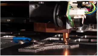
Joule 3D printing from Digital Alloys. Image courtesy of Digital Alloys.
So, instead, we might consider a joule heating-powered method akin to what Digital Alloys offers. We could begin with a metal substrate, onto which all of the phone will be printed. As the inkjet or aerosol jet head creates the electronics, a metal deposition head would surge electricity through metal wire and deposit the metal into place around the parts.
Conclusion
As someone without a materials science degree, it seems at least plausible in the distant future to 3D print an entire smartphone in a single build operation. By the time it’s doable, we might have an atom configuring technology that is even simpler. More likely, we can imagine a more complex system, involving an assembly line of printers and robots.
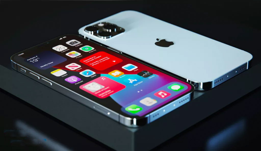
The iPhone 13 from Apple. Image courtesy of Apple.
When the possibility of 3D printing smartphones was being explored by Google and 3D Systems, the process was similar to the PrintValley technology developed by Dutch research institute TNO. A train of print beds would move on a racetrack-like conveyance system from station to station, as materials are deposited and cured and functional elements are installed into place.
The way that such a process is shown on the TNO machine above makes it look like this could be almost immediately achievable. Given that it was developed a decade ago makes that seem even more possible. If so, then the problem would be more of a matter of business and economics.
Currently, it makes more sense to mass manufacture individual components around the world and have them assembled at a central location where labor is cheap. Until that is no longer the case, we can imagine Apple adopting specific 3D printing technologies.
Maybe Aerosol Jet would be used to fabricate more geometrically complex antennas directly onto phone components. A battery printing technology, if it exists, could make smaller, denser energy storage solutions. PCB 3D printing could be used to prototype chips in-house. And, of course, plastic sintering could be used to produce custom phone cases.
Meanwhile, 3D printing could be used more and more frequently by third parties to develop specialty modules for their smartphones. This offers the greatest possibilities in the science and medical spaces, where researchers have already developed a number of smartphone-based tools for diagnosing illnesses and measuring environmental data.
So, does Apple have 3D printers in-house? Most certainly. Is it using them to produce smartphones? At least at the research and development level. Is it possible to 3D print an iPhone? Technically possible, but the business case for such a scenario is unlikely.
Subscribe to Our Email Newsletter
Stay up-to-date on all the latest news from the 3D printing industry and receive information and offers from third party vendors.
You May Also Like
Precision at the Microscale: UK Researchers Advance Medical Devices with BMF’s 3D Printing Tech
University of Nottingham researchers are using Boston Micro Fabrication‘s (BMF) 3D printing technology to develop medical devices that improve compatibility with human tissue. Funded by a UK grant, this project...
3D Printing Webinar and Event Roundup: April 21, 2024
It’s another busy week of webinars and events, starting with Hannover Messe in Germany and continuing with Metalcasting Congress, Chinaplas, TechBlick’s Innovation Festival, and more. Stratasys continues its advanced training...
3D Printing Webinar and Event Roundup: March 17, 2024
It’s another busy week of webinars and events, including SALMED 2024 and AM Forum in Berlin. Stratasys continues its in-person training and is offering two webinars, ASTM is holding a...
3D Printed Micro Antenna is 15% Smaller and 6X Lighter
Horizon Microtechnologies has achieved success in creating a high-frequency D-Band horn antenna through micro 3D printing. However, this achievement did not rely solely on 3D printing; it involved a combination...